
Highlights Nano Materials
In the NanoNextNL program a number of projects was started and lead to innovative science and application. Below you will find a number of examples of projects from the NanoNextNL program.
Writing electrical contacts on sensitive materials
NanoNextNL PhD researcher Adrie Mackus has developed a gentle way of very accurately producing components such as electrical contacts on sensitive materials such as graphene. Graphene is a highly promising material for the even faster and smaller electronics of the future. With the current methods for producing electrical contacts on chips you destroy the graphene, however. Project partner and electron microscope manufacturer FEI has applied for a patent on the new writing method.
‘The plastic of the 21st-century’ is how graphene is often referred to. The material, which consists of a single atomic layer of carbon atoms in a characteristic honeycomb structure, could signify a revolution within electronics. It is extremely strong, exceptionally hard and conducts electricity better than copper. It could, for example, be used to produce flexible screens or for very powerful computer chips. But in order to do that you must be able to make electrical contacts on it. And with the current technology that is not yet possible. NanoNextNL PhD researcher Adrie Mackus has developed a method that is suitable for making very precise contacts on such sensitive materials.
For the current silicon-based computer chips manufacturers such as Intel make use of lithographic techniques to produce different layers with electronic components and connections: you place a thin film of the material on the silicon surface, stick a light-sensitive lacquer layer to this, illuminate that layer with the desired pattern and subsequently etch away the unwanted material of the thin film with aggressive chemicals. For sensitive nanomaterials such as graphene and carbon nanotubes this method for creating patterns is not an option, however. The chemicals corrode these materials, as a result of which they lose their functionality.
‘About 25% of a solar panel’s costs arise from the material costs of the silicon used,’ says Frank Lenzmann. ‘Therefore with the help of smart technology we are trying to ensure that we need less silicon to produce a solar cell that is at least as efficient.’ In addition there is an environmental benefit: silicon is extracted from sand where it occurs in the form of silicon dioxide. You need high temperatures to make pure silicon from this. During the process, CO2 is also released. Therefore the less silicon you need, the less harmful the production process is for the environment. However, even the current solar panels generate electricity in a far more environmentally friendly manner than coal and gas-fired power stations.
Laborious
Furthermore, this method is in all honesty highly laborious says Mackus’ supervisor Erwin Kessels from Eindhoven University of Technology: ‘Imagine you were to build a house in this manner. Then you would build a complete cube of bricks and then subsequently remove the majority of those bricks with the exception of the walls. We are searching for ways of simply building just the walls for the structures and chips.’
Combination
In his NanoNextNL project PhD researcher Adrie Mackus combined two existing techniques to directly write patterns on the surface. With an electron beam he first wrote thin lines of platinum. The beam of electrons was targeted at gaseous platinum compounds that were scattered across the surface. Only the platinum particles located in the path of the beam were deposited on the surface. Next he used a technique called atomic layer deposition (ALD) to build walls of platinum on top of the lines. Atomic layer deposition uses gases to be able to deposit materials atomic layer by atomic layer on top of pre-defined locations. Up until Mackus’ research this method was mainly used to deposit complete films of materials and not so much for making thin lines.
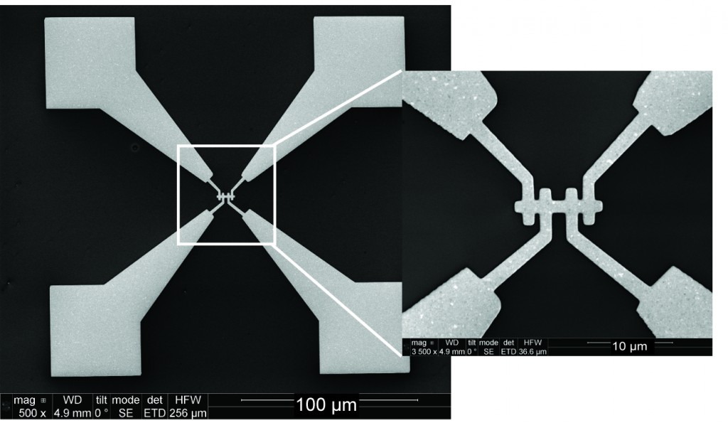
Using a combination of techniques, Adrie Mackus managed to write neat electrical contacts of just a few micrometres in size directly on a surface.
Promise
Due to the major breakthrough that Mackus has managed to achieve with his approach he received his doctorate cum laude in 2013. Since then he has been a postdoc at the prestigious Stanford University. Meanwhile the researchers in Eindhoven have been working further on refining the technology, says Kessels: ‘With this technique you can make platinum contacts on chips but you can also build other nanostructures. If you want to make components with new materials such as graphene then, in principle, such a writing process works better than lithography. An approach such as that of Adrie combines the best properties of the two techniques used. And although I do not want to pretend that we have now found the final solution, I nevertheless have high expectations for it.’
Read more
News item promotion Adrie Mackus
Thesis Adrie Mackus
Nanoparticles to order
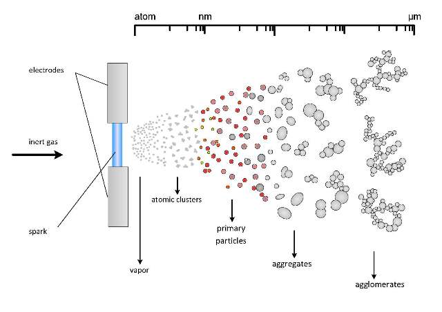
Produce very clean, identical nanoparticles for efficient catalysts or for miniature electronics – all in single step. VSParticle, a young start-up from Delft University of Technology with a well-filled cabinet of prizes, can do just that. With a Valorisation Grant from NanoNextNL and a Take-off loan from Technology Foundation STW, founders Aaike van Vugt and Tobias Pfeiffer are now conquering the market. Future clients range from scientific researchers to chip and printer manufacturers.
Nanoparticles are used in many different applications, ranging from batteries to electronics and from catalysts to printers. However, how do you make such particles with dimensions one-hundred-thousandth the thickness of a human hair, and that all have the same size and exactly the same composition to boot?
The Delft start-up company VSParticle has developed a new technology for this, which can produce nanoparticles and deposit these on a surface in a single step and without the need for any extra chemicals. With their patented technology, the founders of the company won several prizes in its first year, from the New Venture Prize and a Valorisation Voucher from the European organisation Climate-KIC, to a three-month stay at MIT to participate in the worldwide Global Founders’ Skills Accelerator.
Printing electronics
Originally, the founders of VSParticle wanted to focus on the research market, but they rapidly discovered that this technology was interesting for many other markets as well, says Van Vugt. ‘For example, we are in discussion with parties in the electronics industry, who want to print lines of metal. In order to do that, you need printer heads that can apply very small nanoparticles in a pattern on a surface. And with our technology, we can take care of that quite easily.’ ‘Our company is the result of 15 years of research at Delft University of Technology,’ says CEO Aaike van Vugt. ‘Using our technology, it is easier and cheaper to make better nanoparticles than you can with the standard processes that have been used for this up to now. We have built a first version of our device, and we will further develop it using the NanoNextNL Valorisation Grant and the Take-off grant.’
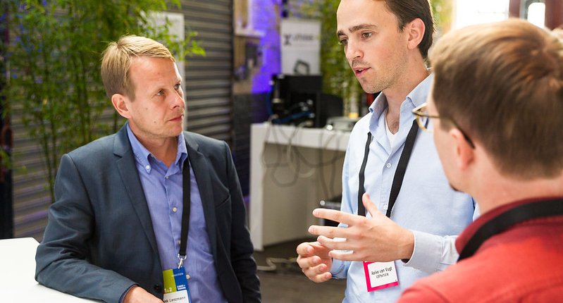
Aaike van Vugt (CEO VSParticle) presented his company during NanoCity 2015
Simple solution
He shows the device concerned, which truly emanates a ‘Keep it simple’ vision. The box, which easily fits on a table, includes two buttons, a gas inlet and an outlet the particles emerge from. ‘When somebody purchases such a particle generator from us, they are also given a training in which we explain all the possibilities. They can then make almost anything they could come up with.’
Current processes to produce the particles are often based on chemical principles. For example, the particles are linked to a solvent that needs to be removed in subsequent steps. This requires extra process steps and introduces contaminants in the particles. ‘Our technology is entirely physical in nature. We incorporate the material you want to make nanoparticles of into two electrodes. By placing a high voltage across these, we create a very brief and hot spark that causes the material to evaporate. This is a very rapid process, which yields very pure nanoparticles of every desired composition. And you are immediately done, as no purifying post-treatment processes are necessary.’
Read more
Article ‘Groter groeien met de kleinste deeltjes’ (fd.nl – in Dutch only)
From chance discovery to wound healing plaster
A gel that becomes stiff if it warms up and fluid if it cools down. This counterintuitive material was discovered by NanoNextNL researchers from Radboud University Nijmegen several years ago while they were searching for something else. Now after a publication in Nature and several patents, the start-up Secmatix is busy developing the gel for medical applications.
Chemists Paul Kouwer, Alan Rowan and postdoc Mattieu Koepf discovered a gel that is elastic, non-toxic and has small holes that are permeable to water and air but not bacteria. The gel also has a structure similar to biological tissues, as a result of which it can be used as a scaffold for the growth of new cells.
Spray-on plaster
You could use this to produce a spray-on plaster. The plaster would stiffen due to the body’s own heat and would therefore completely seal a wound. You would not have to damage anything when removing the plaster, as you would simply place the affected body area briefly under a cold tap. The plaster would become fluid again and simply drip off. Alternatively, you could use the gel as a structure in the laboratory to culture human tissues in 3D, such as parts of organs.
At the end of 2014 a large project was started, Heal-X. In this collaborative project the possibility of using the hydrogel to treat burns better is being investigated.
Application areas
These two applications form the first focus areas of the company Secmatix, which was founded at the end of 2014 to commercialise the gel. In addition to the examples already mentioned various other potential application areas are currently being investigated. For example, at the end of 2014 a large project called Heal-X was awarded funding by the Netherlands Organisation for Health Research and Development (ZonMw). In this collaborative project with Radboud University Nijmegen, RadboudUMC, the Association of Dutch Burn Centres, the Brandwondenstichting (Dutch Burns Foundation) and Chiralix the possibility of using the hydrogel to treat burns better is being investigated.
Future
The company envisages a big future for the gel based on the unique properties of the material. Years of research have provided a firm foundation. The gel’s properties have been investigated under various conditions and the first toxicity tests in mice have been completed. Now it is down to Secmatix in conjunction with the researchers to choose the application areas with the greatest potential, to bring the right people together to work further on these, and to realise funding and large-scale production.
Cheaper catalyst by using less platinum
Platinum, an expensive noble metal, is an important component of catalytic convertors in cars. The less of it you need, the cheaper your catalytic convertor is to produce. The company Delft Intensified Materials Production (Delft IMP) uses a technology that can deposit materials atomic layer by atomic layer to produce the same quality catalyst for catalytic convertors with 35 percent less platinum.
‘Our technology can indeed be used to very accurately and energy-efficiently produce catalysts in powder form for use in car exhausts,’ says CEO Bart van Limpt of the fledgling company that is a spin-off of Delft University of Technology. ‘Platinum lies at the heart of these catalysts. With our method, we can very accurately apply thin layers of platinum to grains of a cheap carrier material. This approach requires 35 percent less platinum than the current processes. As the production cost of a catalyst is largely determined by the cost of the platinum, our approach can considerably reduce the price of catalysts.’
From battery to pigment
The same technique can also be used in a wide range of other applications. One example is coating lithium-ion battery particles with aluminium oxide to ensure that the battery particles degrade less quickly; this increases the lifespan of such a battery. Another example is covering pigments with a thin transparent protective layer so that they do not lose their colour under the influence of sunlight or water.
Demonstration
Van Limpt attends congresses with a simple model that he uses to demonstrate how the technology works. Small spherical particles in a glass tray are brought into motion using nitrogen gas. The individual spheres can be uniformly coated by allowing the coating in gaseous form to pass through the glass tray. ‘We use a specific chemistry that ensures you always get the same final product. This works better than the wet chemistry often used at present, in which various substances are mixed together in their liquid phase and you are left hoping that the same chemical reaction occurs throughout the entire mixture.’
The technology is based on a technique called atomic layer deposition (ALD). ALD is already used widely in the semiconductor industry but we introduce this technology to the process industry for the first time. With this process we can coat kilograms per hour instead of several grams per hour.
From semiconductors to process industry
The technology is based on a technique called atomic layer deposition (ALD). This technique is already used widely in the semiconductor industry to very accurately apply various materials layer-by-layer to silicon wafers. ‘We are now introducing this technology to the process industry for the first time,’ says Van Limpt. The fledgling company has already received a Valorisation Grant from NanoNextNL and a Take-Off Grant from STW, and it also reached the top-10 of the European ClimateLaunchpad, a competition for highly promising cleantech start-ups.
Scaling up
The process has emerged from the academic research performed by Ruud van Ommen of Delft University of Technology. He developed and patented a way of scaling up the ALD process, which can normally coat several grams of material per hour at the lab scale, into a fully-fledged production facility that can coat kilograms per hour. ‘With the help of the Valorisation Grant, we will construct this pilot-scale system to show potential clients the strength of the technology,’ says Van Limpt.
Many advantages
The entrepreneur is a convincing promoter of his product’s many benefits. ‘Catalysts are often made using expensive components. With our technology, we can obtain the same efficacy with a far smaller quantity of the expensive material. Furthermore, this technology does not require high temperatures and produces very few undesired by-products. This means that besides reducing costs, our technology is also far more environmentally friendly than the current production methods. This technology can be used nearly universally. As soon as our pilot-scale reactor has been built, we will show a wide range of manufacturers what our technology could mean for their company by using our reactor to produce their specific product according to their specific requirements.’
Read more
Nano4Society Foundation
![]()
University of Twente
Hallenweg 15
7522 NH Enschede
The Netherlands

